Five-bit R-2R DAC in VLSI
Simulated 2026
I never fabricated it, and the full die with the pad frame hasn't been through DRC or LVS, so this is layout plus simulation.
A 5-bit R-2R DAC drawn as a chip layout in Electric VLSI, with the netlist pulled back out of the layout and simulated in LTspice against the ideal ladder across all 32 codes.
The ladder
It’s a 5-bit voltage-mode R-2R ladder with no op-amp, run from 5 V. One step is 156.25 mV, so the top code (11111) gives 4.84375 V. There are 16 resistors, all 10k, because each 2R is just two 10k resistors in series. In the layout they’re n-well resistors.
Looking back into the output, the resistance is R (10k) for every code, and the open-circuit voltage is 5 times the code over 32.
The layout
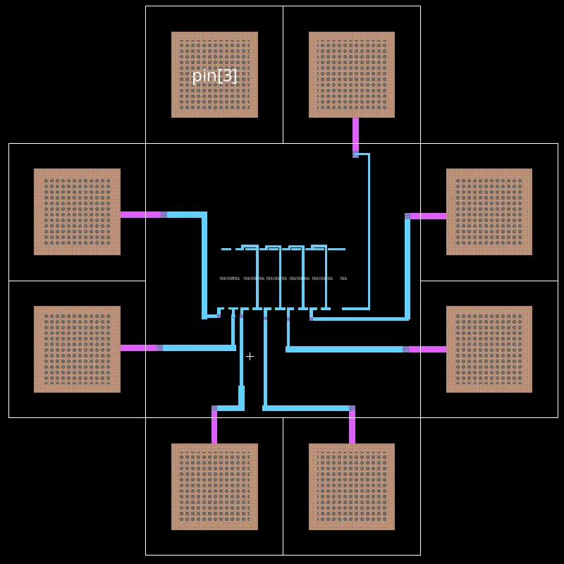
I drew one resistor cell, an n-well strip 164 units long and 14 wide in Electric’s units, sized from R = Rsheet x L / W after checking the n-well and contact rules. Three of them make a divider, and the DAC is five dividers plus one more resistor, with pins for b0 to b4, vout and ground. I worked in Electric on the MOSIS technology and checked everything in LTspice.
Does the layout match the schematic
I pulled a netlist out of the layout and ran the same sweep three ways: the ideal ladder, the LTspice schematic and the extracted layout. All 32 codes agree to six decimals. Code 31 is 4.843750 V in all three.
That tells me the layout is wired like the schematic. It doesn’t tell me the resistors would be accurate in silicon, because the extracted netlist still uses ideal 10k resistors with no process variation.
Loading and speed
The output impedance is 10k, so it wants a load much bigger than that. A 10k load halves the output: code 31 drops to 2.421875 V.
Into 10 pF, with a 0 to 2 V step on the top bit, the simulated 50% delay is 69.52 ns. By hand, tau = RC = 100 ns, and 0.7 RC is 70 ns.
The pad frame
The second lab wraps the DAC in a frame of 8 bonding pads, two per side, 1600 by 1600 units. The DAC’s seven pins go to seven pads and the spare pad (pin 3) is left unconnected.