FPGA implementation
I targeted a Xilinx Zynq-7000 on a Digilent PYNQ-Z2 board for hardware bring-up. This page documents what synthesis cost, where the timing closed, where the design sat on the fabric, and the live demo running on the board. The bug from bring-up moved to the Verification postmortems, where it shares context with the rest of the verification work.
Toolchain and target
- Target board: Xilinx Zynq-7000 (PYNQ-Z2)
- Toolchain: Vivado 2025.2
- Top module:
src/pynq_z2_top.sv - Clock target: 10 MHz (period 100 ns, closed with positive slack)
Resource utilization
The full RV32I core, register file, instruction and data memories, MMIO, and the PYNQ-Z2 top-level fit comfortably in the Zynq-7000 with substantial headroom for future extensions (caches, additional MMIO, peripherals).
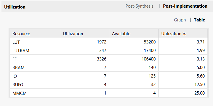 Vivado post-implementation utilization for the full design.
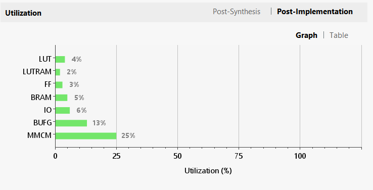 Same utilization, broken out by module hierarchy: the register file and ALU dominate, the memories are small.
Timing closure
The clock was constrained to 100 ns (10 MHz). At that target Vivado closes with positive worst-negative-slack across all paths; the timing summary below is the post-implementation report.
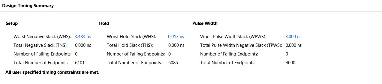 Setup, hold, and pulse-width all met at 10 MHz.
Fmax is open. The 10 MHz constraint was deliberately conservative for bring-up; rerunning synthesis with the constraint loosened (or removed) and reading the resulting WNS would let me quote a real maximum. That’s a TODO; until I do, the fmax card in the results strip at the top of this page stays hidden.
Implementation layout
The placed-and-routed design on the Zynq-7000 fabric, captured from the Vivado device view. The placement is sparse, which is the visual confirmation of the utilization numbers above.
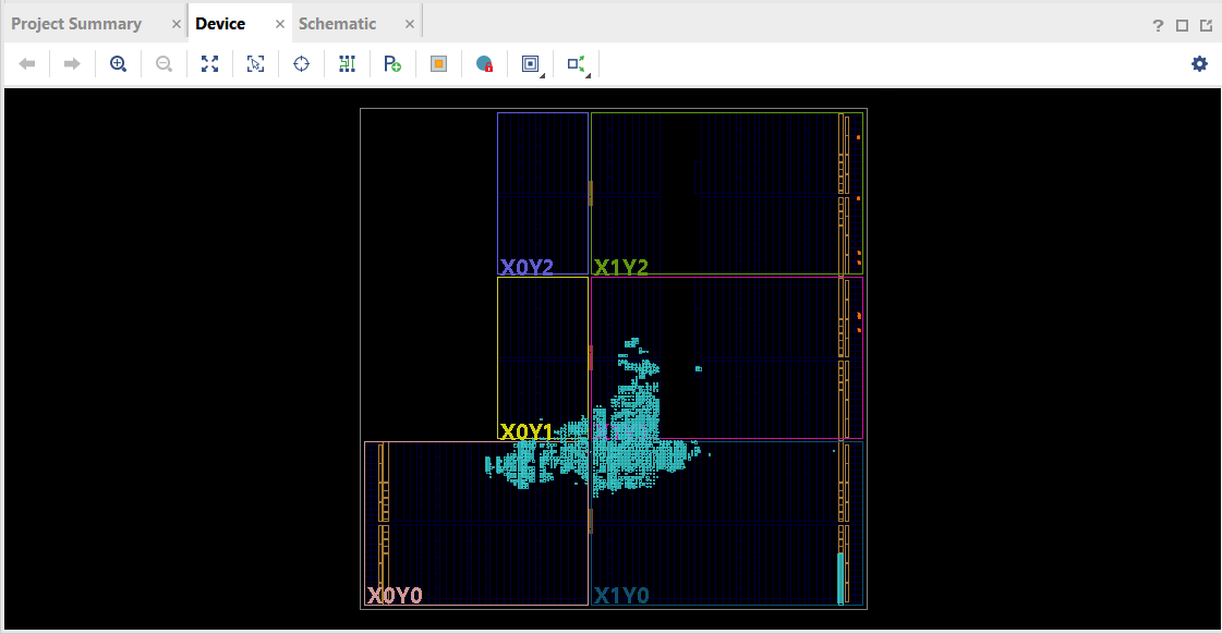 Post-implementation placement on the Zynq-7000 fabric. The lit-up region shows the riscv-5i core; the rest of the device is unused.
Lessons from bring-up
Two pieces of advice I would give myself if I were starting again:
- Use the Xilinx Clocking Wizard for any non-trivial clock. The first revision of the PYNQ-Z2 top-level used a small logic-based clock divider to derive the CPU clock from the board’s 125 MHz reference. That worked in simulation, but on the board the JTAG debug hub became unstable and the ILA dropped triggers intermittently. Switching to a Clocking Wizard IP block stabilized the clock tree, fixed the JTAG flakiness, and made the ILA reliable. Worth the IP-block bureaucracy.
- Memory timing is the first thing to verify on real hardware. The bug documented in the postmortem was a sim-vs-synth mismatch: the simulation model of the instruction memory was combinational, the FPGA implementation used synchronous block RAM. The pipeline’s IF stage assumes single-cycle fetch, and that assumption only failed on the board. Anything that simulates one way and synthesizes another deserves an explicit equivalence check before bring-up.
Hardware demo
src/pynq_z2_top.sv wires the lower four bits of the MMIO LED register at 0x8000_0000 to the board’s four user LEDs. Any RISC-V program that writes to that address shows up on the LEDs the next cycle. The demo program is a Fibonacci generator that writes successive terms; because the LEDs are four bits, values larger than 15 wrap modulo 16, so the visible sequence rolls over after 13, 21, 34.
Sequence Displayed on LEDs:
  * 1  -> 0001 (1)
  * 2  -> 0010 (2)
  * 3  -> 0011 (3)
  * 5  -> 0101 (5)
  * 8  -> 1000 (8)
  * 13 -> 1101 (13)
  * 21 -> 0101 (5)  (21 is 10101 binary; bottom 4 bits are 0101)
  * 34 -> 0010 (2)  (34 is 100010 binary; bottom 4 bits are 0010)
A short video of the program running on the board. The same Fibonacci binary that produces this sequence on hardware also passes its regression testbench in simulation.
Reproducing the build
- Bitstream and synthesis scripts live under
fpga/in the repo. - The Fibonacci hex image used above:
test/mem/fib_test.mem. - End-to-end build steps (Vivado project generation, bitstream, board flash): Setup.